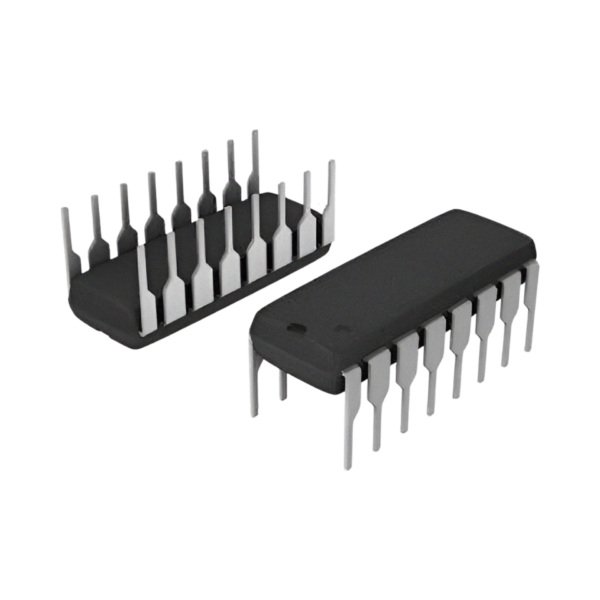
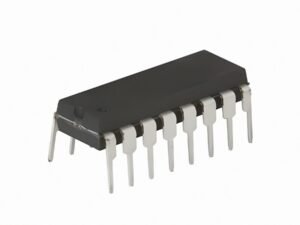
Table: Overview of 4052 IC (Dual 4-Channel Analog Multiplexer/Demultiplexer)
| Parameter | Description/Value |
|---|---|
| Part Number | 4052 |
| Function | Dual 4-Channel Analog Multiplexer/Demultiplexer |
| Logic Family | CMOS |
| Supply Voltage (Vdd) | 3V to 15V |
| Maximum Switching Frequency | 40 MHz (at 10V supply) |
| Typical Propagation Delay | 150 ns at 5V |
| Operating Temperature Range | -55°C to +125°C |
| Pin Count | 16 |
| Package Types | PDIP, SOIC, TSSOP, QFN |
| Output Type | Buffered |
| Input Type | CMOS Compatible |
| Power Dissipation | Low Power Consumption |
| On-Resistance | 80Ω (Typical) at Vdd=10V |
| Off-Channel Leakage Current | ±0.1nA (Typical) at Vdd=10V |
| Analog Voltage Range | 0V to Vdd |
| Applications | Signal routing, data acquisition, audio switching |
| Datasheet Reference | CD4052B, HCF4052, MC14052B |
| Pin Configuration | 1: Y1; 2: Y0; 3: Z; 4: VEE; 5: Y2; 6: Y3; 7: Z’; 8: Vss (Ground); 9: A; 10: B; 11: Enable; 12: X; 13: W; 14: X’; 15: Vdd (Supply Voltage) |
Detailed Description
The 4052 IC is a dual 4-channel analog multiplexer/demultiplexer that operates across a wide range of supply voltages from 3V to 15V. It belongs to the CMOS logic family, known for its low power consumption and high noise immunity. The IC allows the multiplexing or demultiplexing of analog signals, with each channel being independently controlled. This makes it suitable for applications such as signal routing, data acquisition, and audio switching.
Pin Functions
- Y0 to Y3 (Pins 2, 1, 5, 6): Analog channels for the first multiplexer/demultiplexer.
- Z, Z’ (Pins 3, 7): Common outputs/inputs for the first and second multiplexer/demultiplexer.
- VEE (Pin 4): Negative power supply pin (often connected to ground in single-supply configurations).
- Vss (Pin 8): Ground pin.
- A, B (Pins 9, 10): Channel select inputs.
- Enable (Pin 11): Enable input (active low).
- X, X’ (Pins 12, 14): Common outputs/inputs for the second multiplexer/demultiplexer.
- W (Pin 13): Analog channel for the second multiplexer/demultiplexer.
- Vdd (Pin 15): Positive supply voltage pin.
Electrical Characteristics
- Input Voltage High (Vih): 3.5V (Min) at Vdd=5V
- Input Voltage Low (Vil): 1.5V (Max) at Vdd=5V
- On-Resistance: 80Ω (Typical) at Vdd=10V
- Off-Channel Leakage Current: ±0.1nA (Typical) at Vdd=10V
The 4052 IC is widely used in digital and analog applications that require reliable signal switching and routing due to its high performance and flexibility in multiplexing/demultiplexing operations.
Pinout Table for 4052 IC
| Pin Number | Pin Name | Description |
| 16 | Vdd | Positive power input, maximum 20V |
| 7 | Vee | Negative power rail, normally connected to ground. |
| 8 | Vss (Ground) | Connected to ground of the circuit |
| 6 | INH | Enable pin – Must be pulled to ground for normal operation |
| 9,10 | A,B | Channel Select pins |
| 1,12 | Y0,X0 | Channel 0 Input / Output |
| 5,14 | Y1,X1 | Channel 1 Input / Output |
| 2,15 | Y2,X2 | Channel 2 Input / Output |
| 4,11 | Y3,X3 | Channel 3 Input / Output |
| 3,13 | Y,X | Common Output / Input |


Reviews
There are no reviews yet.