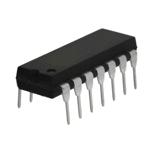
Table: Overview of 4047 IC (Monostable/Astable Multivibrator)
| Parameter | Description/Value |
|---|---|
| Part Number | 4047 |
| Function | Monostable/Astable Multivibrator |
| Logic Family | CMOS |
| Supply Voltage (Vdd) | 3V to 15V |
| Maximum Frequency (Astable Mode) | 1.5 MHz (at 10V supply) |
| Typical Propagation Delay | 125 ns at 5V |
| Operating Temperature Range | -55°C to +125°C |
| Pin Count | 14 |
| Package Types | PDIP, SOIC, TSSOP |
| Output Type | Buffered |
| Input Type | CMOS Compatible |
| Power Dissipation | Low Power Consumption |
| Reset Function | Asynchronous |
| Clock Input | Edge-triggered |
| Quiescent Current | 1 µA (Typical) at 5V |
| High-Level Output Voltage (Voh) | 4.95V (Min) at Vdd=5V, Io=-1µA |
| Low-Level Output Voltage (Vol) | 0.05V (Max) at Vdd=5V, Io=1µA |
| Applications | Timer, oscillator, pulse generation, frequency division |
| Datasheet Reference | CD4047B, HCF4047, MC14047B |
| Pin Configuration | 1: Astable; 2: A; 3: B; 4: Reset; 5: Cext; 6: Rext/Cext; 7: Rext; 8: Vss (Ground); 9: Q; 10: !Q; 11: !Q2; 12: Q2; 13: Trigger; 14: Vdd (Supply Voltage) |
Detailed Description
The 4047 IC is a versatile monostable/astable multivibrator that operates across a wide range of supply voltages from 3V to 15V. It belongs to the CMOS logic family, known for its low power consumption and high noise immunity. The IC can be configured to operate in either monostable (one-shot) or astable (oscillating) mode, making it suitable for applications such as timers, oscillators, pulse generation, and frequency division.
Pin Functions
- Astable (Pin 1): Controls astable mode operation.
- A (Pin 2): External timing resistor input.
- B (Pin 3): External timing capacitor input.
- Reset (Pin 4): Asynchronous reset input.
- Cext (Pin 5): External capacitor input for timing.
- Rext/Cext (Pin 6): Combined external resistor and capacitor input for timing.
- Rext (Pin 7): External resistor input for timing.
- Vss (Pin 8): Ground pin.
- Q (Pin 9): Output in astable mode and pulse output in monostable mode.
- !Q (Pin 10): Complementary output of Q.
- !Q2 (Pin 11): Complementary output for the second Q.
- Q2 (Pin 12): Second output in astable mode.
- Trigger (Pin 13): Trigger input for starting the monostable mode.
- Vdd (Pin 14): Positive supply voltage pin.
Electrical Characteristics
- Input Voltage High (Vih): 3.5V (Min) at Vdd=5V
- Input Voltage Low (Vil): 1.5V (Max) at Vdd=5V
- Output Voltage High (Voh): 4.95V (Min) at Vdd=5V, Io=-1µA
- Output Voltage Low (Vol): 0.05V (Max) at Vdd=5V, Io=1µA
Pinout Table for 4047 IC
| Pin Number | Pin Name | Description |
|---|---|---|
| 1 | Astable | Controls astable mode operation |
| 2 | A | External timing resistor input |
| 3 | B | External timing capacitor input |
| 4 | Reset | Asynchronous reset input |
| 5 | Cext | External capacitor input for timing |
| 6 | Rext/Cext | Combined external resistor and capacitor input for timing |
| 7 | Rext | External resistor input for timing |
| 8 | Vss | Ground |
| 9 | Q | Output in astable mode and pulse output in monostable mode |
| 10 | !Q | Complementary output of Q |
| 11 | !Q2 | Complementary output for the second Q |
| 12 | Q2 | Second output in astable mode |
| 13 | Trigger | Trigger input for starting the monostable mode |
| 14 | Vdd | Positive supply voltage |


Reviews
There are no reviews yet.