Attributes
Table: Overview of 4027 IC (Dual J-K Master-Slave Flip-Flop)
| Parameter | Description/Value |
|---|---|
| Part Number | 4027 |
| Function | Dual J-K Master-Slave Flip-Flop |
| Logic Family | CMOS |
| Supply Voltage (Vdd) | 3V to 15V |
| Maximum Clock Frequency | 12 MHz (at 10V supply) |
| Typical Propagation Delay | 125 ns at 5V |
| Operating Temperature Range | -55°C to +125°C |
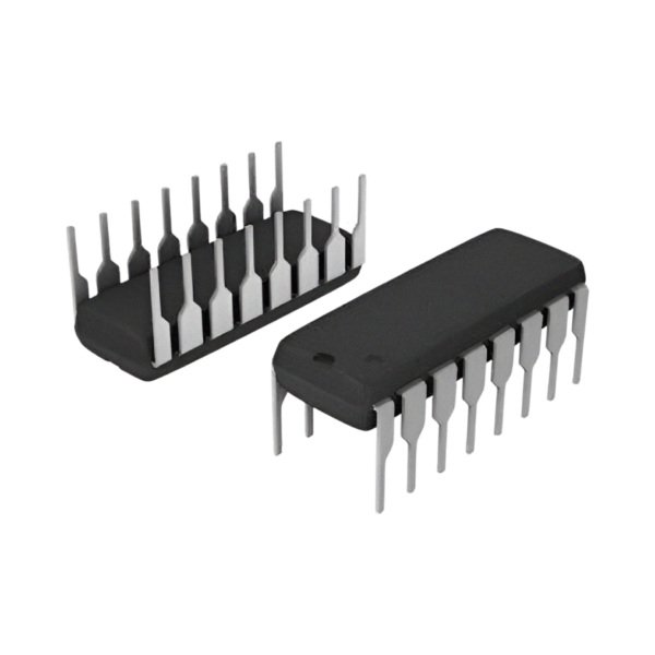
| Pin Count | 16 |
| Package Types | PDIP, SOIC, TSSOP |
| Output Type | Buffered |
| Input Type | CMOS Compatible |
| Power Dissipation | Low Power Consumption |
| Reset Function | Asynchronous |
| Clock Input | Edge-triggered |
| Quiescent Current | 10 nA (Typical) at 5V |
| High-Level Output Voltage (Voh) | 4.95V (Min) at Vdd=5V, Io=-1µA |
| Low-Level Output Voltage (Vol) | 0.05V (Max) at Vdd=5V, Io=1µA |
| Applications | Data storage, frequency division, toggle operations |
| Datasheet Reference | CD4027B, HCF4027, MC14027B |
Detailed Description
The 4027 IC is a dual J-K master-slave flip-flop that operates across a wide range of supply voltages from 3V to 15V. As part of the CMOS logic family, it offers low power consumption and high noise immunity. The IC features two independent J-K flip-flops, each with set and reset inputs, making it suitable for a variety of applications including data storage, frequency division, and toggle operations.
Pin Functions
- Q1 (Pin 1): Output of the first flip-flop.
- !Q1 (Pin 2): Complementary output of the first flip-flop.
- Q2 (Pin 3): Output of the second flip-flop.
- !Q2 (Pin 4): Complementary output of the second flip-flop.
- J2 (Pin 5): J input of the second flip-flop.
- K2 (Pin 6): K input of the second flip-flop.
- Clock2 (Pin 7): Clock input for the second flip-flop.
- Vss (Pin 8): Ground pin.
- R2 (Pin 9): Reset input for the second flip-flop (active high).
- S2 (Pin 10): Set input for the second flip-flop (active high).
- S1 (Pin 11): Set input for the first flip-flop (active high).
- R1 (Pin 12): Reset input for the first flip-flop (active high).
- Clock1 (Pin 13): Clock input for the first flip-flop.
- K1 (Pin 14): K input of the first flip-flop.
- J1 (Pin 15): J input of the first flip-flop.
- Vdd (Pin 16): Positive supply voltage pin.
Electrical Characteristics
- Input Voltage High (Vih): 3.5V (Min) at Vdd=5V
- Input Voltage Low (Vil): 1.5V (Max) at Vdd=5V
- Output Voltage High (Voh): 4.95V (Min) at Vdd=5V, Io=-1µA
- Output Voltage Low (Vol): 0.05V (Max) at Vdd=5V, Io=1µA
Pinout Table for 4027 IC
| Pin Number | Pin Name | Description |
|---|---|---|
| 1 | Q1 | Output of the first flip-flop |
| 2 | !Q1 | Complementary output of the first flip-flop |
| 3 | Q2 | Output of the second flip-flop |
| 4 | !Q2 | Complementary output of the second flip-flop |
| 5 | J2 | J input of the second flip-flop |
| 6 | K2 | K input of the second flip-flop |
| 7 | Clock2 | Clock input for the second flip-flop |
| 8 | Vss | Ground |
| 9 | R2 | Reset input for the second flip-flop (active high) |
| 10 | S2 | Set input for the second flip-flop (active high) |
| 11 | S1 | Set input for the first flip-flop (active high) |
| 12 | R1 | Reset input for the first flip-flop (active high) |
| 13 | Clock1 | Clock input for the first flip-flop |
| 14 | K1 | K input of the first flip-flop |
| 15 | J1 | J input of the first flip-flop |
| 16 | Vdd | Positive supply voltage |


Reviews
There are no reviews yet.