Attributes
Table: Overview of 4025 IC (Triple 3-Input NOR Gate)
| Parameter | Description/Value |
|---|---|
| Part Number | 4025 |
| Function | Triple 3-Input NOR Gate |
| Logic Family | CMOS |
| Supply Voltage (Vdd) | 3V to 15V |
| Maximum Input Frequency | 8 MHz (at 10V supply) |
| Typical Propagation Delay | 60 ns at 5V |
| Operating Temperature Range | -55°C to +125°C |
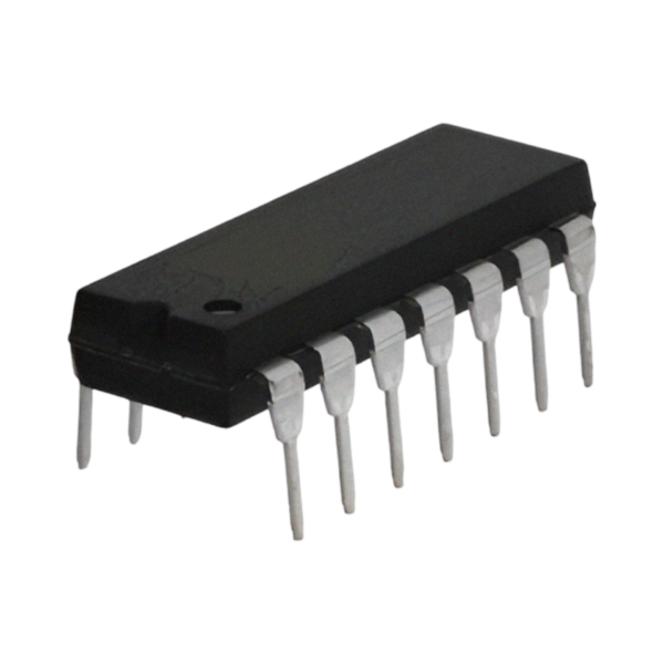
| Pin Count | 14 |
| Package Types | PDIP, SOIC, TSSOP |
| Output Type | Buffered |
| Input Type | CMOS Compatible |
| Power Dissipation | Low Power Consumption |
| Logic Level | NOR Gate Functionality |
| Quiescent Current | 1 µA (Typical) at 5V |
| High-Level Output Voltage (Voh) | 4.95V (Min) at Vdd=5V, Io=-1µA |
| Low-Level Output Voltage (Vol) | 0.05V (Max) at Vdd=5V, Io=1µA |
| Applications | Logic circuits, digital design, signal inversion |
| Datasheet Reference | CD4025B, HCF4025, MC14025B |
| Pin Configuration | 1: A1; 2: B1; 3: C1; 4: Q1; 5: A2; 6: B2; 7: C2; 8: Vss (Ground); 9: Q2; 10: A3; 11: B3; 12: C3; 13: Q3; 14: Vdd (Supply Voltage) |
Detailed Description
The 4025 IC is a versatile triple 3-input NOR gate that operates across a wide range of supply voltages from 3V to 15V. It belongs to the CMOS logic family, known for its low power consumption and high noise immunity. Each of the three NOR gates within the IC can process three inputs to produce a single output, following the NOR gate logic function. This IC is used in various digital logic applications, including logic circuits, digital design, and signal inversion.
Pinout
| Pin Number | Pin Name | Description |
|---|---|---|
| 1 | A1 | Input A of the first NOR gate |
| 2 | B1 | Input B of the first NOR gate |
| 3 | C1 | Input C of the first NOR gate |
| 4 | Q1 | Output of the first NOR gate |
| 5 | A2 | Input A of the second NOR gate |
| 6 | B2 | Input B of the second NOR gate |
| 7 | C2 | Input C of the second NOR gate |
| 8 | Vss | Ground |
| 9 | Q2 | Output of the second NOR gate |
| 10 | A3 | Input A of the third NOR gate |
| 11 | B3 | Input B of the third NOR gate |
| 12 | C3 | Input C of the third NOR gate |
| 13 | Q3 | Output of the third NOR gate |
| 14 | Vdd | Positive supply voltage |
Pin Functions
- A1, B1, C1 (Pins 1, 2, 3): Inputs for the first NOR gate.
- Q1 (Pin 4): Output of the first NOR gate.
- A2, B2, C2 (Pins 5, 6, 7): Inputs for the second NOR gate.
- Q2 (Pin 9): Output of the second NOR gate.
- A3, B3, C3 (Pins 10, 11, 12): Inputs for the third NOR gate.
- Q3 (Pin 13): Output of the third NOR gate.
- Vdd (Pin 14): Positive supply voltage pin.
- Vss (Pin 8): Ground pin.
Electrical Characteristics
- Input Voltage High (Vih): 3.5V (Min) at Vdd=5V
- Input Voltage Low (Vil): 1.5V (Max) at Vdd=5V
- Output Voltage High (Voh): 4.95V (Min) at Vdd=5V, Io=-1µA
- Output Voltage Low (Vol): 0.05V (Max) at Vdd=5V, Io=1µA


Reviews
There are no reviews yet.