Attributes
| Parameter | Description | Value |
|---|---|---|
| Supply Voltage (Vcc) | Operating voltage range | 4V to 12V |
| Quiescent Current (Icc) | Current drawn when amplifier is not amplifying | 4 mA |
| Output Power | Maximum output power to the load (8 ohms) at Vcc = 9V | 700 mW |
| Voltage Gain | Adjustable gain range by external resistors and capacitors | 20 to 200 |
| Bandwidth | Frequency response bandwidth (typically) | 300 kHz |
| Input Impedance | Impedance at the input terminal | 50 kΩ |
| Output Impedance | Impedance at the output terminal | 10 Ω |
| Input Bias Current | Typical input bias current | 250 nA |
| Total Harmonic Distortion (THD) | Distortion of the output signal (at 1 kHz) | 0.2% |
| Slew Rate | Rate at which output voltage can change | 0.5 V/μs |
| Operating Temperature | Range of temperatures over which the device operates effectively | 0°C to 70°C |
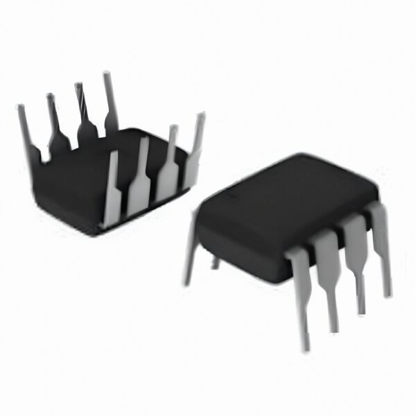
| Package | Physical packaging types available | DIP-8, SOIC-8 |
| Noise Figure | Level of noise generated by the amplifier | 2 μV |
| PSRR (Power Supply Rejection Ratio) | Ratio of the change in output voltage to the change in the supply voltage | 50 dB |
| Common Mode Rejection Ratio (CMRR) | Ratio of common mode signal to differential signal rejection | 80 dB |
Pin Configuration
| Pin Number | Pin Name | Description |
|---|---|---|
| 1 | Gain | Connects to an external capacitor to set the gain (default gain is 20 if left unconnected) |
| 2 | Inverting Input | The inverting input terminal of the amplifier |
| 3 | Non-inverting Input | The non-inverting input terminal of the amplifier |
| 4 | GND | Ground |
| 5 | Output | Output terminal for the amplified signal |
| 6 | Vcc | Power supply terminal |
| 7 | Bypass | Bypass terminal for an external capacitor to reduce power supply noise |
| 8 | Gain | Connects to an external capacitor to set the gain (in conjunction with Pin 1, default gain is 20 if left unconnected) |
Download


Reviews
There are no reviews yet.