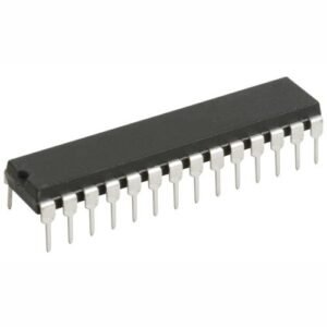
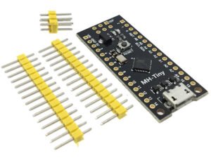
Microcontroller from Atmel AVR 28-leg DIP case. Voltage supply ranges from 2.7 V to 5.5 V, frequency up to 16 MHz, has 8 KB Flash, 1 KB RAM, and 512 B of EEPROM.
Specifications:
| Product Attribute | Attribute Value |
| Product Category: | 8-bit Microcontrollers – MCU |
| Core: | AVR |
| Program Memory Size: | 8 kB |
| Data RAM Size: | 1 kB |
| Package/Case: | PDIP-28 |
| Maximum Clock Frequency: | 16 MHz |
| ADC Resolution: | 10 bit |
| Number of I/Os: | 23 I/O |
| Supply Voltage – Min: | 2.7 V |
| Supply Voltage – Max: | 5.5 V |
| Mounting Style: | Through Hole |
| Data Bus Width: | 8 bit |
| Minimum Operating Temperature: | – 40 C |
| Maximum Operating Temperature: | + 85 C |
| Series: | ATmega8A |
| Data RAM Type: | SRAM |
| Data ROM Size: | 512 B |
| Data ROM Type: | EEPROM |
| Interface Type: | SPI, TWI, USART |
| Number of ADC Channels: | 6 Channel |
| Number of Timers/Counters: | 3 Timer |
| Program Memory Type: | Flash |
Pin Configurations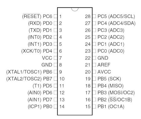
ATMEGA8 Pin Configuration
| Pin No. | Pin name | Description | Alternate Function |
| 1 | PC6 (RESET) | Pin6 of PORTC | Pin by default is used as RESET pin. If the RSTDISBL Fuse is programmed, PC6 can be used as an I/O pin.
(Pulled HIGH to RESET controller) |
| 2 | PD0 (RXD) | Pin0 of PORTD | RXD (USART Input Pin)
USART Serial Communication Interface [Can be used for programming] |
| 3 | PD1 (TXD) | Pin1 of PORTD | TXD (USART Output Pin)
USART Serial Communication Interface [Can be used for programming] INT2( External Interrupt 2 Input) |
| 4 | PD2 (INT0) | Pin2 of PORTD | External Interrupt INT0 |
| 5 | PD3 (INT1) | Pin3 of PORTD | External Interrupt INT1 |
| 6 | PD4 (XCK/T0) | Pin4 of PORTD | T0( Timer0 External Counter Input)
XCK ( USART External Clock I/O) |
| 7 | VCC | ||
| 8 | GND | ||
| 9 | PB6 (XTAL1/TOSC1) | Pin6 of PORTB | XTAL1 (Chip Clock Oscillator pin 1 or External clock input)
TOSC1 (Timer Oscillator pin 1) |
| 10 | PB7 (XTAL2/TOSC2) | Pin7 of PORTB | XTAL2 (Chip Clock Oscillator pin 2)
TOSC2 (Timer Oscillator pin 2) |
| 11 | PD5 (T1) | Pin5 of PORTD | T1(Timer1 External Counter Input) |
| 12 | PD6 (AIN0) | Pin6 of PORTD | AIN0(Analog Comparator Positive I/P) |
| 13 | PD7 (AIN1) | Pin7 of PORTD | AIN1(Analog Comparator Negative I/P) |
| 14 | PB0 (ICP1) | Pin0 of PORTB | ICP1(Timer/Counter1 Input Capture Pin) |
| 15 | PB1 (OC1A) | Pin1 of PORTB | OC1A (Timer/Counter1 Output Compare Match A Output) |
| 16 | PB2 (SS/OC1B) | Pin2 of PORTB | SS (SPI Slave Select Input). This pin is low when controller acts as slave.
[Serial Peripheral Interface (SPI) for programming] OC1B (Timer/Counter1 Output Compare Match B Output) |
| 17 | PB3 (MOSI/OC2) | Pin3 of PORTB | MOSI (Master Output Slave Input). When controller acts as slave, the data is received by this pin. [Serial Peripheral Interface (SPI) for programming]
OC2 (Timer/Counter2 Output Compare Match Output) |
| 18 | PB4 (MISO) | Pin4 of PORTB | MISO (Master Input Slave Output). When controller acts as slave, the data is sent to master by this controller through this pin.
[Serial Peripheral Interface (SPI) for programming] |
| 19 | PB5 (SCK) | Pin5 of PORTB | SCK (SPI Bus Serial Clock). This is the clock shared between this controller and other system for accurate data transfer.
[Serial Peripheral Interface (SPI) for programming] |
| 20 | AVCC | Vcc for Internal ADC Converter | |
| 21 | AREF | Analog Reference Pin for ADC | |
| 22 | GND | GROUND | |
| 23 | PC0 (ADC0) | Pin0 of PORTC | ADC0 (ADC Input Channel 0) |
| 24 | PC1 (ADC1) | Pin1 of PORTC | ADC1 (ADC Input Channel 1) |
| 25 | PC2 (ADC2) | Pin2 of PORTC | ADC2 (ADC Input Channel 2) |
| 26 | PC3 (ADC3) | Pin3 of PORTC | ADC3 (ADC Input Channel 3) |
| 27 | PC4 (ADC4/SDA) | Pin4 of PORTC | ADC4 (ADC Input Channel 4)
SDA (Two-wire Serial Bus Data Input/Output Line) |
| 28 | PC5 (ADC5/SCL) | Pin5 of PORTC | ADC5 (ADC Input Channel 5)
SCL (Two-wire Serial Bus Clock Line) |


Reviews
There are no reviews yet.