Product Details
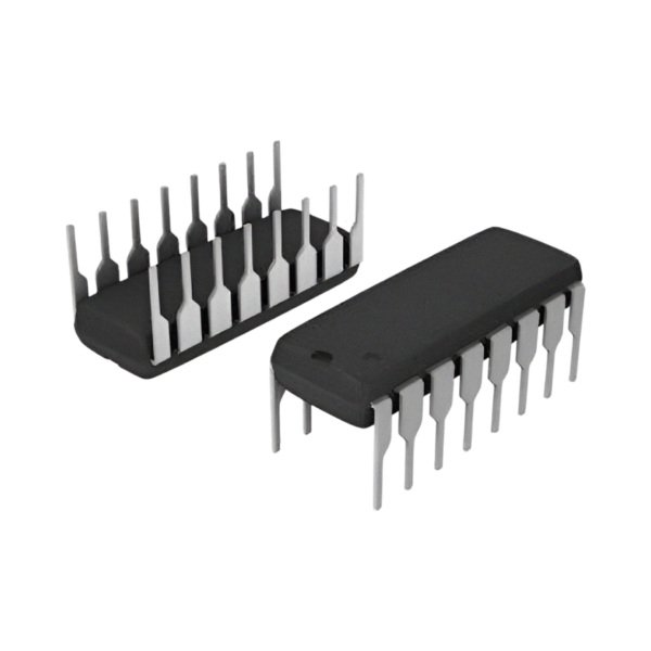
The 7476 IC or IC 7476 is a Dual, Separate Positive-Edge Triggered J-K Flip-Flop. With separate J-K inputs, as well as individual Clock, Preset and Clear Inputs. For the 7476 IC Flip-Flops, the input to the J-K pins is moved into the master when the clock signal is HIGH. The data is then transferred to the slave when the clock transitions from HIGH to LOW. The 7476 pin diagram or 7476 pinout is shown below.
Features
- Two J-K Master-Slave Flip-Flops with Preset and Clear Inputs
- Outputs Directly Interface to CMOS, NMOS and TTL
- Large Operating Voltage Range
- Wide Operating Conditions
Pin Layout

Pin Description
| Pin Number | Description |
|---|---|
| 1 | Clock 1 Input |
| 2 | Preset 1 Input |
| 3 | Clear 1 Input |
| 4 | J1 Input |
| 5 | Vcc – Positive Power Supply |
| 6 | Clock 2 Input |
| 7 | Preset 2 Input |
| 8 | Clear 2 Input |
| 9 | J2 Input |
| 10 | Complement Q2 Output |
| 11 | Q2 Output |
| 12 | K2 Input |
| 13 | Ground |
| 14 | Complement Q1 Output |
| 15 | Q1 Output |
| 16 | K1 Input |
Dimensional Drawing

Technical Data
Absolute Maximum Ratings
| Supply Voltage | 7V |
| Input Voltage | 5.5V |
| Operating Free Air Temperature | 0°C to +70°C |
| Storage Temperature Range | -65°C to +150°C |
Recommended Operating Conditions
| Symbol | Parameter | Min | Typ | Max | Units |
|---|---|---|---|---|---|
| Vcc | Supply Voltage | 4.75 | 5 | 5.25 | V |
| Vih | HIGH Level Input Voltage | 2 | V | ||
| Vil | LOW Level Input Voltage | 0.8 | V | ||
| Ioh | HIGH Level Output Current | -0.4 | mA | ||
| Iol | LOW Level Output Current | 16 | mA | ||
| Ta | Free Air Operating Temperature | 0 | 70 | °C |
Electrical Characteristics
| Symbol | Parameter | Conditions | Min | Typ | Max | Units |
|---|---|---|---|---|---|---|
| Vi | Input Clamp Voltage | Vcc=Min Ii=-12mA | -1.5 | V | ||
| Voh | HIGH Level Output Voltage | Vcc=Min Ioh=MAX Vil=MAX | 2.4 | 3.4 | V | |
| Vol | LOW Level Output Voltage | Vcc=Min Iol=MAX Vih=MAX | 0.2 | 0.4 | V | |
| Ii | Input Current@MAX Input Voltage | Vcc=Max Vi=5.5V | 1 | mA | ||
| Iih | HIGH Level Input Current | Vcc=Max Vi=2.4V | 40 | µA | ||
| Iil | LOW Level Input Current | Vcc=Max Vi=0.4V | -1.6 | mA | ||
| Ios | Short Circuit Output Current | Vcc=Max | -18 | -55 | mA | |
| Icch | Supply Current with Outputs HIGH | Vcc=Max | 4 | 8 | mA | |
| Iccl | Supply Current with Outputs LOW | Vcc=Max | 12 | 22 | mA |
Switching Characteristics at Vcc=5V,Ta=25°C
| Symbol | Parameter | Conditions | Min | Typ | Max | Units |
|---|---|---|---|---|---|---|
| tplh | Propagation Delay Time LOW-to-HIGH Level Output | Cl=15pF Rl=400R | 22 | nS | ||
| tphl | Propagation Delay Time HIGH-to-LOW Level Output | Cl=15pF Rl=400R | 15 | nS |


Reviews
There are no reviews yet.