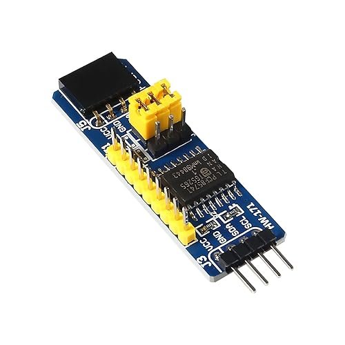
PCF8574 I2C I/O Expansion Module
The PCF8574 I²C I/O Expansion Module is designed to extend the input/output capabilities of microcontrollers through the I²C interface. It provides 8 quasi-bidirectional GPIO pins (P0–P7), allowing each pin to function as either an input or output without the need for a separate data-direction control signal. This flexibility makes it suitable for various applications, including driving LEDs, reading switches, and interfacing with sensors.
The module features an open-drain interrupt output (via INT pin), enabling efficient monitoring of input changes without continuous polling. Multiple PCF8574 modules can be connected on the same I²C bus, with configurable addresses (via A0–A2 pins) allowing up to 8 devices, thereby expanding the I/O count to 64. Its low power consumption and compatibility with 3.3 V and 5 V systems make it an excellent choice for embedded and battery-powered applications.
Features
Adds 8 digital I/O pins via I2C interface with PCF8574.
Quasi-bidirectional I/O pins configurable as inputs or outputs.
Open-drain interrupt output for efficient input change detection.
Supports up to 8 devices on the same I2C bus with configurable addresses.
Low standby current consumption, suitable for low-power applications.
Compatible with 3.3V and 5V logic levels.
High-current drive capability for directly driving LEDs.
No need for separate data-direction control signals.
Compact module size for easy integration into projects.
Ideal for expanding GPIO in microcontroller-based systems.
Specifications
Parameter Details
Operating Voltage 2.5 V–6 V
Standby Current < 10 µA
I/O Pins 8 quasi-bidirectional
I2C Address Configurable Yes, via A0–A2 pins (up to 8 devices)
Interrupt Output Open-drain, active LOW
I2C Interface Speed Up to 100 kHz (Standard-mode)
Logic Level Compatibility 3.3 V and 5 V systems
Output Drive Capability High-current drive for LEDs
Package Types Various (e.g., SOIC, PDIP, TSSOP)
Pin Function
A0 Address bit 0: tie to GND (0) or VCC (1) to set the least significant address bit (value = 1).
A1 Address bit 1: tie to GND (0) or VCC (1) to set the next address bit (value = 2).
A2 Address bit 2: tie to GND (0) or VCC (1) to set the next address bit (value = 4).
GND Ground reference, common with microcontroller ground.
VCC Power supply (2.5 V – 6 V), typically 3.3 V or 5 V
SDA I²C data line (open-drain), requires pull-up resistor to VCC.
SCL I²C clock line (open-drain), requires pull-up resistor to VCC.
INT Open-drain interrupt output (active LOW). Goes LOW when any input-configured pin (P0–P7) changes state; cleared by reading or writing the I/O ports.
P0 Quasi-bidirectional I/O pin 0: can function as input (with internal pull-up) or output (driving LOW or HIGH as float).
P1 Quasi-bidirectional I/O pin 1: same operation as P0.
P2 Quasi-bidirectional I/O pin 2: same operation as P0.
P3 Quasi-bidirectional I/O pin 3: same operation as P0.
P4 Quasi-bidirectional I/O pin 4: same operation as P0.
P5 Quasi-bidirectional I/O pin 5: same operation as P0.
P6 Quasi-bidirectional I/O pin 6: same operation as P0.
P7 Quasi-bidirectional I/O pin 7: same operation as P0; unused pins should be configured as outputs to prevent floating.
Note: Unused P0–P7 pins should be configured as outputs (e.g., write LOW) to prevent floating inputs and reduce power consumption.
Applications
Expanding GPIO for microcontrollers with limited I/O pins.
Driving LEDs, relays, and other output devices.
Reading inputs from switches, buttons, and sensors.
Implementing keypad interfaces.
Home automation systems.
Industrial control and monitoring.
Embedded systems requiring additional I/O.
Battery-powered applications needing low standby current.
Projects requiring multiple I/O expanders on a single I2C bus.
Educational and prototyping platforms.
Package Contents
1x PCF8574 I2C I/O Expansion Module.


Reviews
There are no reviews yet.