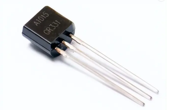
Specification and Features
|
Characteristic |
Value/Range |
|
Type |
PNP |
|
Maximum Collector Power Dissipation (Pc) |
0.4 W (Watts) |
|
High Voltage and High Current |
Vceo = 50V, Ic = 150mA |
|
Low Noise |
1 dB |
|
Case Material |
Molded Plastic |
|
DC Current Gain (hfe) |
70 to 400 |
|
Collector-Base Voltage (Vcb) |
-50 V |
|
Collector-Emitter Voltage (Vce) |
-50 V |
|
Emitter-Base Voltage (Veb) |
-5 V |
|
Maximum Collector Current (Ic max) |
-150 mA |
|
Max. Operating Junction Temperature (Tj) |
150 °C |
|
Transition Frequency (ft) |
80 MHz |
|
Complementary Transistor |
2SC1815 |
A1015 Transistor Pinout Description:
-
Emitter (E)
Pin Number: 1
Description: The emitter is the terminal through which the transistor’s collector current exits. It is also the lead through which current flows into the transistor when it’s in the active state. In PNP transistors like the A1015, the emitter is typically connected to the most negative voltage level (negative with respect to the collector) in the circuit. Current flows from the emitter to the collector when the transistor is in its active mode.
-
Collector (C)
Pin Number: 2
Description: The collector is where the transistor’s collector current enters the device. It plays a crucial role in controlling the flow of current between the emitter and collector. The collector is typically connected to the positive supply voltage in PNP transistors. When the base current is applied to the transistor, it allows current to flow from the emitter to the collector, thus amplifying or switching the input signal.
-
Base (B)
Pin Number: 3
Description: The base terminal is responsible for controlling the transistor’s operation. When a small current is applied to the base, it regulates the much larger current flowing from the emitter to the collector. By controlling the base current, you can switch the transistor between its “off” and “on” states. In amplification applications, a small change in the base current results in a much larger change in collector current, making the transistor suitable for signal amplification.
A1015 Transistor Circuit Diagram
-
A1015 Transistor Amplifier
The diagram illustrates an amplifier circuit using A1015 and C1815 transistors.
This is a push-pull AB class amplification circuit composed of two transistors as amplifying components and two antiparallel diodes to achieve complementary operation.
When an audio signal is fed into the circuit, it is initially bypassed by an input capacitor. Subsequently, the signal undergoes amplification through the two transistors. The push-pull operation of A1015 and C1815 transistors results in a substantial amplification of the audio signal, taking into account the signal’s characteristics.
-
LED flasher using 2SA1015
In the circuit illustrated below, we’ve employed a 2SA1015 transistor in an LED flasher application. Here’s how it operates:
Capacitor C1 and resistor R1 work in tandem to generate a specific frequency, which is then supplied to the base of transistor Q1. Q1 serves as a switch that controls the behavior of Q2. Q2, in turn, is responsible for amplifying the current. The process unfolds as follows:
Initially, the voltage builds up across C1. During this phase, Q1 remains active, facilitating the flow of current through R2 and the LED. As the voltage across C1 continues to rise, it eventually reaches a point where Q2 starts to conduct. At this juncture, a current begins to flow through the LED, causing it to illuminate.
As C1 gradually discharges through R1 over a specified period, it reaches a point where it can no longer provide bias to the base terminal of Q1. Consequently, Q1 ceases to function, leading to the deactivation of Q2. This, in turn, causes the LED to switch off.
With the LED turned off, C1 begins the process anew, setting off a continuous cycle. This on-off sequence of the LED creates the flashing effect, making it appear as a flasher.


Reviews
There are no reviews yet.