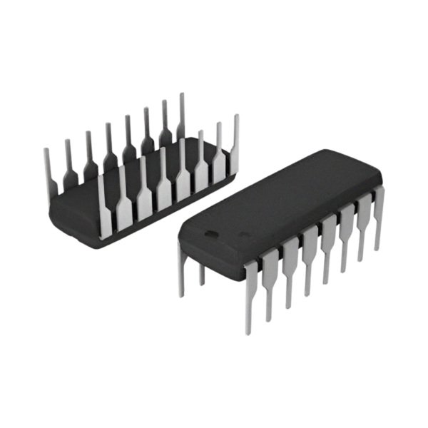
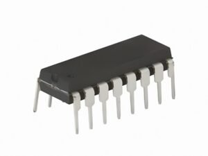
Table: Overview of 4040 IC (12-Stage Binary Ripple Counter)
| Parameter | Description/Value |
|---|---|
| Part Number | 4040 |
| Function | 12-Stage Binary Ripple Counter |
| Logic Family | CMOS |
| Supply Voltage (Vdd) | 3V to 15V |
| Maximum Clock Frequency | 12 MHz (at 10V supply) |
| Typical Propagation Delay | 200 ns at 5V |
| Operating Temperature Range | -55°C to +125°C |
| Pin Count | 16 |
| Package Types | PDIP, SOIC, TSSOP |
| Output Type | Buffered |
| Input Type | CMOS Compatible |
| Power Dissipation | Low Power Consumption |
| Reset Function | Asynchronous Master Reset |
| Clock Input | Edge-triggered |
| Quiescent Current | 10 nA (Typical) at 5V |
| High-Level Output Voltage (Voh) | 4.95V (Min) at Vdd=5V, Io=-1µA |
| Low-Level Output Voltage (Vol) | 0.05V (Max) at Vdd=5V, Io=1µA |
| Applications | Frequency division, event counting, time delay generation |
| Datasheet Reference | CD4040B, HCF4040, MC14040B |
| Pin Configuration | 1: Reset; 2: Q12; 3: Q11; 4: Q10; 5: Q9; 6: Q8; 7: Q7; 8: Vss (Ground); 9: Q6; 10: Q5; 11: Q4; 12: Q3; 13: Q2; 14: Q1; 15: Clock; 16: Vdd (Supply Voltage) |
Detailed Description
The 4040 IC is a versatile 12-stage binary ripple counter that operates across a wide range of supply voltages from 3V to 15V. It is part of the CMOS logic family, known for its low power consumption and high noise immunity. The IC features an asynchronous master reset, allowing the counter to be reset at any time. The clock input is edge-triggered, making it suitable for counting pulses in various applications such as frequency division, event counting, and time delay generation.
Pin Functions
- Reset (Pin 1): Asynchronous reset input that resets all stages of the counter when held high.
- Q12 to Q1 (Pins 2-7, 9-14): Outputs representing the binary count.
- Clock (Pin 15): Clock input used to advance the counter on the rising edge of the clock signal.
- Vdd (Pin 16): Positive supply voltage pin.
- Vss (Pin 8): Ground pin.
Electrical Characteristics
- Input Voltage High (Vih): 3.5V (Min) at Vdd=5V
- Input Voltage Low (Vil): 1.5V (Max) at Vdd=5V
- Output Voltage High (Voh): 4.95V (Min) at Vdd=5V, Io=-1µA
- Output Voltage Low (Vol): 0.05V (Max) at Vdd=5V, Io=1µA
Pinout Table for 4040 IC
| Pin Number | Pin Name | Description |
|---|---|---|
| 1 | Reset | Asynchronous reset input |
| 2 | Q12 | Output for the 12th stage |
| 3 | Q11 | Output for the 11th stage |
| 4 | Q10 | Output for the 10th stage |
| 5 | Q9 | Output for the 9th stage |
| 6 | Q8 | Output for the 8th stage |
| 7 | Q7 | Output for the 7th stage |
| 8 | Vss | Ground |
| 9 | Q6 | Output for the 6th stage |
| 10 | Q5 | Output for the 5th stage |
| 11 | Q4 | Output for the 4th stage |
| 12 | Q3 | Output for the 3rd stage |
| 13 | Q2 | Output for the 2nd stage |
| 14 | Q1 | Output for the 1st stage |
| 15 | Clock | Clock input |
| 16 | Vdd | Positive supply voltage |


Reviews
There are no reviews yet.